
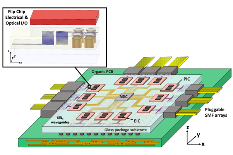
An MIT-led research program aimed at creating future microsystems capable of sustainably transmitting data with greater bandwidth and higher efficiency than is possible today, has made several significant advances since it was established in 2022.
These include the invention of devices within systems that can much more easily integrate electronics—manipulating data with electricity—with photonics, which does the same with light. The microsystems, the first of their kind, also promise to be cost-effective because, among other advantages, they can be manufactured using existing equipment in traditional electronics foundries and packaging houses.
“Our disruptive electronic-photonic integrated solutions will enable us to leap from [transmitting data at] 100s of terabits per second to greater than 1 petabit per second,” said Anu Agarwal, who leads MIT’s FUTUR-IC. An advanced system using co-packaged optics can provide improved bandwidth and energy savings compared to what is used today, which is electronics-only or pluggable optics.
Agarwal, a principal research scientist at the Materials Research Laboratory, was speaking at an April webinar titled, “Shaping the Future of Semiconductors: Power, Performance, and Possibility.” The event was sponsored by the MIT Industrial Liaison Program and Startup Exchange.
Toward Sustainability
The microchips behind everything from smart phones to medical imaging can be traced to about 500 megatons of CO2-equivalent lifetime emissions in 2021 that is predicted to exceed 100 million metric tons under a business-as-usual scenario, and every year the world produces more than 50 million tons of electronic waste. Further, the huge data centers necessary for complex computations like on-demand video, are growing and will require close to ten percent of the world’s electricity by 2030.
“This is neither scalable nor sustainable, and cannot continue,” Agarwal has re-iterated over the years. FUTUR-IC, funded by the National Science Foundation Convergence Accelerator, was created to address these resource-efficiency issues.
For example, integrating photonics with the electronics that underpin today’s microchips could address energy use because the transmission, or communication of data, using light is much more energy efficient. “Our mantra is to use electronics for computation and photonics for communication to bring this energy crisis under control,” said Agarwal.
Currently, however, it is difficult and expensive to connect electronic chips with their photonic counterparts within a single package. That’s partly because the supply-chain ecosystem for co-packaged optics is still immature.
New Devices
Enter two new devices developed through FUTUR-IC aimed at making it easier—and less expensive—to integrate photonic chips with microchips. One, the evanescent coupler, was featured on the cover of Advanced Engineering Materials last year. Another, known as the graded index coupler (GRIN) was reported in the March 2026 print issue of the Journal of Physics: Photonics.
A third new coupler was developed by an MIT team led by Professor Juejun Hu of the Department of Materials Science and Engineering. It was reported in a 2023 issue of Laser & Photonics Reviews. That work was supported by the Department of Energy.
The three couplers are the first optical equivalents of the “solder bumps,” or tiny dots of metal that allow chip-to-chip or chip-to-substrate connections for electron flow. Until this MIT work, there were no analogous “optical bump” options for photonics.
And if photonics is to be integrated with electronics, “you’ll need both metal bumps and optical bumps because there are devices on your photonics chip that will require both an electrical signal and an optical signal,” says Drew Weninger, first author of the papers on both the evanescent and GRIN couplers. Weninger, MIT PhD 2025, is now at the National Institute of Standards and Technology.
As with electronics, many options of optical bumps will be necessary, as “each type has substantial tradeoffs,” write Weninger and colleagues in a review article in Nature about coupler advances published earlier this year.
For example, the GRIN coupler can be used over a wider spectrum of light than is possible with the evanescent coupler, Weninger says. The evanescent coupler, however, is easier to fabricate and can be packed in tighter to form a higher number of connections.
Additional Advances
FUTUR-IC is organized into three dimensions: Technology (the coupler work is a good example), Value Chain Innovation, and Workforce.
Under the Value Chain sector, Agarwal described a new tool to support companies’ decisions toward sustainability. Earthster provides a visual model for quickly determining the energy, materials usage, and environmental sustainability across a company’s products. For example, said Agarwal, “Looking at [Earthster], a supplier can tell right away their hot spots for carbon emissions and start working to minimize them.”
FUTUR-IC has also developed several programs aimed at the development of a future workforce for next-generation microchips. For example, “it is introducing an online course on semiconductor resource efficiency,” Agarwal said. “Our education team at the MIT Initiative for Knowledge and Innovation in Manufacturing (IKIM) also offers gamified digital learning and problem-based learning, plus a Summer Academy and a hands-on bootcamp.” For K-12 awareness, FUTUR-IC has created Ted-Ed videos.
Agarwal concluded her April webinar by acknowledging the range of industries FUTUR-IC aims to help. “If you’re a packaging vendor, a materials vendor, or you are in the supply chain for data centers, FUTUR-IC can provide value.”
Additional authors of the paper on the GRIN coupler are Agarwal; Lionel Kimerling, the Thomas Lord Professor in the Department of Materials Science and Engineering (DMSE); Christian Duessel, MIT BS 2025 now at SiLC Technologies, a silicon photonics company, and Samuel Serna, professor of physics, photonics and optical engineering at Bridgewater State University.
Additional authors of the Nature review paper are Serna; Luigi Ranno, MIT PhD 2025 now at Ayar Labs; Kimerling, and Agarwal.