
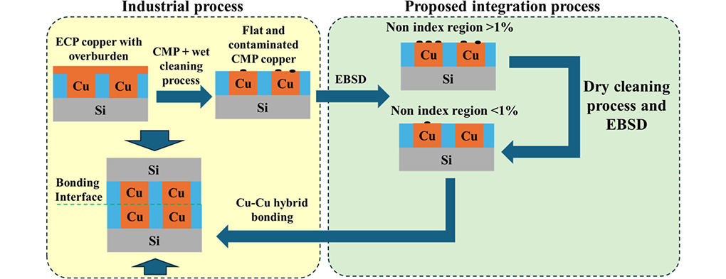
Abstract— Achieving clean and smooth copper (Cu) surfaces is critical for reliable Cu-to-Cu hybrid bonding in advanced semiconductor packaging. Secondary electron microscopy, equipped with an electron backscattered diffraction (EBSD) detector, is proposed as the primary detection technique to assess the structural and crystallographic properties by quantifying crystallinity, grain quality, and amorphous content of Cu pads during cleaning processes following chemical-mechanical polishing (CMP). Because the CMP process introduces both surface (∼1–2 nm) and subsurface (∼1–20 nm) contamination and damage, proper cleaning is essential. In this study, a systematic EBSD framework is developed, and it is shown that varying the incident energy modulates the interaction volume, thereby revealing surface and subsurface information on copper pads. The proposed technique investigates two post-CMP cleaning processes: double forming gas annealing (DFGA) and double deep oxidation (DDO) processes as models. EBSD enables a clear quantitative assessment of the Cu pads’ surface recovery, revealing substantial restoration of crystalline order following the cleaning treatments. The AFM study complements the EBSD results by confirming a significant reduction in surface roughness. At the same time, cross-sectional TEM/STEM-EDS revealed a decrease in the thickness of copper oxy-carbide species (CuOxCy) from ∼50 nm to <5 nm after DDO. These findings establish SEM-EBSD as a powerful, nondestructive, and measurement-driven approach for evaluating Cu pad quality for high-yield hybrid bonding.
 |
Carl V. Thompson
|