
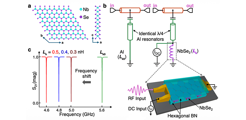
Abstract — Van der Waals (vdW) superconductors remain superconducting down to the monolayer limit, enabling the exploration of emergent physical phenomena and functionality driven by reduced dimensionality. Here, we report the characterization of the kinetic inductance of atomically thin NbSe2, a two-dimensional van der Waals superconductor, using superconducting coplanar waveguides and microwave measurement techniques familiar to circuit quantum electrodynamics (cQED). The kinetic inductance scales inversely with the number of NbSe2 layers, reaching 1.2 nH/□ in the monolayer limit. Furthermore, the measured kinetic inductance exhibits a thickness-dependent crossover from clean- to dirty-limit behavior, with enhanced dirty-limit contributions emerging in the ultra-thin regime. These effects are likely driven by increased surface scattering, multi-band superconductivity, and geometric confinement. Additionally, the self-Kerr nonlinearity of the NbSe2 films ranges from K/2π = −0.006 to −14.7 Hz/photon, indicating its strong potential in applications requiring compact, nearly linear, high-inductance superconducting quantum devices and detectors. The fabrication and characterization techniques demonstrated here are extensible to the investigation of other two-dimensional superconductors.
 |
Pablo Jarillo-Herrero |