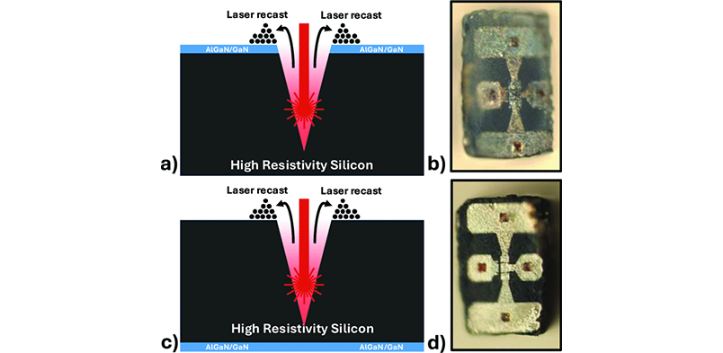
Abstract— With the maturation of III-V semiconductors, such as gallium nitride (GaN), strong use cases for the 3D heterogeneous integration (3DHI) of these technologies with Si CMOS and interposers are emerging in the fields of wireless, power, quantum and photonic applications. This work proposes a fabrication technology that enables the formation of "tiny", single-transistor GaN dielets. For the first time, a method to fabricate sub-mm2 dielets using femtosecond laser dicing is presented. Several of the key challenges associated with such scaled dielets are discussed with key insights presented on post foundry processing, backside via alignment, and optimization of femtosecond laser parameters. Dielets are formed using GlobalFoundries 130GaNRF technology with dielet sizes as small as 195 μm x 400 μm x 140 μm. Integration of the dielets in glass interposer and 3D stacking with Si CMOS is also presented in this work.
 |
Tomas Palacios
|